
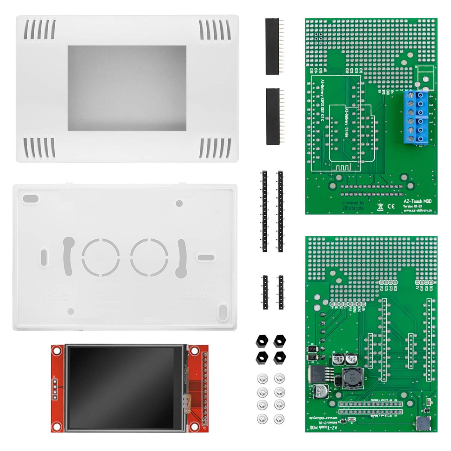
These components are required:
Resistance 3.3 kΩ | 4.7 kΩ | 4x 22 kΩ from the AZ resistor kit
Electrolytic capacitor 10 µF from the AZ Electrolytic Capacitor Set
2 LM 358 operational amplifiers
Electronics retail trade
The idea of this project
After the 6-part contribution to the TDMM has been very well received, I would like to show with this 2-part blog post how you can use the TDMM to measure transistor relationships. This basic knowledge is still of great importance for everyone who develops electronic circuits, even if we today wear millions of transistors in our pocket.
We will equip ourselves with some aids to make these measurements. A D1 Mini V3 works as a ramping generator. A simple measurement amplifier will make our measurement possible (from 0.000001 A).
For a comfortable measurement process controlled by python, we expand the range of functions of the TDMM with further commands. This is one of the advantages of the "Command processor" that we have already installed from the start. Complementing further instructions is very easy.
She learn Know a Python program that automates the measurement processes. This means that you are well equipped to implement your own measurements. In addition, we learn a lot about communication between several computers via USB.
What is a transistor characteristic?
There is a lot of good information on the net, e.g. in Wikipedia or also on the excellent website of Electronics compendium. With their friendly approval, I take over this graphic and can briefly comment on the explanation:
Image 1: Transistor_kennlinienfeld
A transistor (right in the picture) controls the current through its collector emitter route via the base current IB. The base current is about 1/600… 1/900 of the collector current in our Type BC 548C test transistor. The power reinforcement β corresponds to 600… 900 (dimensionless value). A data sheet for this transistor can be found here: BC 548c.
An NPN transistor can be seen in Figure 1. The electricity directions are drawn. IC flows from the positive pole of the power supply by the collector via the emitter to mass.
To the left of the transistor symbol we see a compilation of the four typical characteristics of the transistor characteristic field. We will examine three characteristics more precisely and determine in Part 2.
Tax characteristic
At the top left of the 1st quadrant we see the tax characteristic field in an idealized presentation. It shows the associated collector current for each base current. The slope of the blue line thus reflects the β power reinforcement. A steep line shows a high β, a flat line a lower β.
In practice, we do not find such flawlessly, but yet large, almost ideal areas in which the collector current follows the base current exactly: iC = IB * β.
The input characteristic
Below the tax characteristic field in the 3rd quadrant you can see the input characteristic field. There is the connection between the voltage andbe and the current Ibe again. You may already know this as a typical passage characteristic of a rectifier diode or LED. The tension andbe Between the base and emitter, a certain value must exceed so that a measurable current flows. In silicon, this voltage is around 0.7 V, around 0.3 V.
The starting characteristic field
The 2nd quadrant shows the starting characteristic field. We had seen that a certain iB A defined IC heard. IC but depends on the collector emitter voltage, on uCE. This creates a characteristic of a characteristic with a characteristic for each value of UCE. At first glance you can see that the reinforcement of the transistor is little of uCE depends. This qualifies a transistor with a suitable circuit, for example, for operation as a constant current source.
Our measurements: Quadrant 1 - 3
We limit our measurements to these three quadrants of the characteristic field because the retroactive characteristic (4th quadrant) has less practical importance.
Building the measurements
We determine the following characteristics:
1. Tax characteristic: IB | IC

Figure 2: Measurement of the tax characteristic
For this we measure base current and collector current. The base current flows from the ramping generator through the 100K resistance R5 via the base and the emitter of the transistor to the mass. The ramp generator delivers the base current. Around IB To record, we place the difference amplifier U3a above the 100k resistance. According to the Ohm's law, electricity I calculatesB = UR/R
The differential amplifier has very high -only inputs, so that it hardly falsifies the measurement. UR is the measured voltage on the resistance r (100 kΩ).
We measure the collector current indirectly. To do this, we determine with the TDMM directly on the BC 548C U CollectorCE. The operating voltage of (12 V - uCE) results in the voltage on the 680 ω - resistance from which we iC Received immediately: iC = (12 v - uCE) /680 Ω
2. Starting characteristicCE | IC
For this we measure with the arrangement from 1. For different IB Will Ic in dependence on UCE certainly.
3. Input characteristicbe | IB
We measure the tension andbe directly at the base of the transistor. We also use the difference amplifier for the basic current measurement here.
Our aids: PWM ramp generator and differential amplifier
In addition to the TDMM, we use these two assemblies:
The PWM ramp generator Convert the PWM signal of D1 (PIN 5) of the D1 Mini V3 into a stable DC voltage. We will check whether the DC voltage generated is actually linear Take the PWM signal and descend. I called the assembly "rampenerator" because it is mostly used in practice to create ramp -shaped signals.
The Differential amplifier is a assembly that is widespread in measurement technology. As the name suggests, it reinforces the tension difference between its inputs "+" and "-". He can work invertively, i.e. reverse the signal or non-Invertively, as in our case.
Why do you need such an amplifier? We want to measure the tension over a 100 kΩ resistance. That is why we need a measurement arrangement, the input impedance of which is significantly higher than 100 kΩ. The input impedance of the LM358 is several MΩ, which is completely sufficient for our purposes. There are operational amplifiers with input impedances in the GΩ range.
At the output of the different amplifier we get exactly the signal that is due to its inputs, but with a low output impedance and thus perfectly measurable with the TDMM
Circuit diagram of the PWM ramp generator

Figure 3: circuit diagram of the ramp generator
Useful circuits that can be used again and again, I like to build up on a circuit break and place a connector at one or both ends. In this case, there are two 4-seater pencil strips at each end. You have certainly soldered these strips on your MCUS. I glue the PIN name on the board right away.

Figure 4: The finished ramp generator
The circuit itself is easy to understand. The LM358 contains two surgical amplifiers. The PWM signal from PIN 5 of the D1 Mini V3 comes via a low pass from R1/C1 to the non-Inverting input of the U2A. The operating amplifier is supplied with +12 V. In relation to GND - it can only provide positive signals at its output pin 1.
The second operating amplifier from the 8-legged chip is connected to his outcome. He works as an amplifier. Its reinforcement is calculated from V = 1 +R3/R2. If we set the Poti R3 to zero ohm, the reinforcement = 1. If it is on 10 kΩ, the reinforcement is 1 + 10/3.3, i.e. approx. Factor 4.
Since we receive a PWM signal that corresponds to exactly 3.3 V at a 100% duty ratio, we get a voltage up to 4 x 3.3 V = 13.2 V. Since our circuit cannot represent a "perpetuum mobile" - the output voltage cannot be higher than the input voltage - we need to reinforce> 3 An operating voltage of 15 V. Then this also works.
If we send a PWM signal that gradually increases from 0% to 100% duty ratio (Duty Cycle), we should receive a strictly proportional voltage at the output of the assembly.
Since our measurement can only be as good as our measuring methods and measuring equipment allow it, we want to be the first measurement to send a ramp signal from the D1 Mini V3 and see what comes out of it. The associated sketch is written in two minutes:
Here is the HTML block Insert "rampenerator_test"
int c; // Variable für PWM-Wert
const int pin = 5; // PWM-Pin
void set up() {
pin mode(Pin, output); // set pin 5 as an outcome
}
void loop() {
c = 0;
while (C <256){
Analogwrite(PIN, C);
C ++;
delay(10);
}
analogWrite(pin, 0); // Spannung = 0, Kondensator entladen
delay(500); // Zeit für Kondensatorentladung
}
We can follow the result on an oscilloscope or we increase the delay (10) in the loop and enlarge the increment, for example, to 25, so that you can track a few measurements on the TDMM.

Image 5: linearity check
At first glance, you can see a very excellent linearity between the duty ratio (variable C, left column) and the output voltage. We receive “Pro Digit” on average 26.9 MV output voltage with a scattering of just 100 µV. That is a very good value.
Circuit diagram of the differential amplifier

Image 6: Switch picture_des_ difference
This circuit is easier than for the first assembly. Please use the 22 kΩ resistors from the AZ resistor kit, even if there are 24 kΩ. The exact value is irrelevant. It is important that you use the 1%resistance from the resistor KIT. Otherwise you always have an error signal at the output of the operating amplifier and thus a built -in systematic error.
We get along with an accuracy of a few percent. In professional use, you value a precise zero comparison of the circuit. To do this, you need suitable surgical amplifiers and much more complex circuits that do not offer an advantage for our purposes.

Image 7: Building the difference amplifier
This photo shows the structure on one piece of circuit board. This time I used a 5-pin connector and also labeled it.
The "amplifier" increases exactly 1: 1 - so not at all. What we need is a output voltage related to mass (GND), which is to be measured on the basic resistance of our circuit, but the input signal is not related to mass. The input impedance on the measuring object is very high, the output impedance is very small. You will be able to understand why this is important, because we are now looking at the actual measurement circuit.
Measuring structure for characteristic determination
The actual structure for our measurements is simple and varies only minimally when measuring the different characteristics.

Image 8: Measurement
As a examine, we chose the transistor Q1, a BC548C. It is an often used NPN transistor with a small signal reinforcement in the area of 600 .. 900.
We work with the so -called "emitter circuit". The emitter (pin 3) of the transistor is on mass, the operating voltage of +12 V via the work resistance R4 of 680 Ω on the collector (pin 1).
The signal of our ramp generator is led to the base (PIN 2) via the rather large basic resistance of 100 kΩ. Above the resistance, so to speak "floating" our difference amplifier - only schematically presented here, the complete circuit is meant - the voltage on R5. The base current is calculated from this voltage and the known resistance value (i = u/r).
It's all that simple, but very interesting, which we learn in the measurements that we will go through in detail in the next blog post.
Use of the TDMM for the measurements
We originally programmed the TDMM in such a way that it constantly shows measured values on the display and sends values for U, I and R via the USB interface.
This function turns out to be a hindrance when we carry out our measurements in the transistor. We would like to give the transistor a tension at the base so that a base current flow and determine how to reinforce this current in the collector emitter path.
If constant - uncoordinated - values come from the TDMM, you cannot operate a measurement program with it. We want to set a value and measure the result. Action >> Reaction. But no continuous measurement.
To make this possible, I have expanded our Command processor by three instructions. That has always been an idea for the TDMM: further instructions to be able to add further skills.
I deliver the complete .ino code with this project.
We get these new instructions in the TDMM:
so serial off No more ongoing data output
SA Serial Active ongoing data output
SU Single U Measure Carry out the individual voltage measurement and output the result
We are now prepared to measure the measurements of the input characteristic, output characteristic and To take the tax characteristic. To do this, we expand our sketch for the D1 Mini V3 and write a Python program to control the D1 Mini V3 and the TDMM.
The second blog post deals with the measurements and its evaluation in detail.
Until then,
Best regards
Michael Klein


1 comment
Peter
Hallo,
die 22kΩ/24kΩ Widerstände beim Differenzverstärker sind im Vergleich zum 100kΩ Widerstand an dem der Basisstrom gemessen werden viel zu klein und beeinflussen den Messwert, da sie faktisch wie ein 44kΩ/48kΩ Parallelwiderstand zum 100kΩ Widerstand an der Basis wirken.